Converting blood stem cells to sensory neural cells to predict and treat pain

McMaster University scientists have discovered how to make adult sensory neurons from a patient’s blood sample to measure pain (credit: McMaster University

Stem-cell scientists at McMaster University have developed a way to directly convert adult human blood cells to sensory neurons, providing the first objective measure of how patients may feel things like pain, temperature, and pressure, the researchers reveal in an open-access paper in the journal Cell Reports.

Currently, scientists and physicians have a limited understanding of the complex issue of pain and how to treat it. “The problem is that unlike blood, a skin sample or even a tissue biopsy, you can’t take a piece of a patient’s neural system,” said Mick Bhatia, director of the McMaster Stem Cell and Cancer Research Institute and research team leader. “It runs like complex wiring throughout the body and portions cannot be sampled for study.

“Now we can take easy to obtain blood samples, and make the main cell types of neurological systems in a dish that is specialized for each patient,” said Bhatia. “We can actually take a patient’s blood sample, as routinely performed in a doctor’s office, and with it we can produce one million sensory neurons, [which] make up the peripheral nerves. We can also make central nervous system cells.”

Testing pain drugs

The new technology has “broad and immediate applications,” said Bhatia: It allows researchers to understand disease and improve treatments by asking questions such as: Why is it that certain people feel pain versus numbness? Is this something genetic? Can the neuropathy that diabetic patients experience be mimicked in a dish?

It also paves the way for the discovery of new pain drugs that don’t just numb the perception of pain. Bhatia said non-specific opioids used for decades are still being used today. “If I was a patient and I was feeling pain or experiencing neuropathy, the prized pain drug for me would target the peripheral nervous system neurons, but do nothing to the central nervous system, thus avoiding addictive drug side effects,” said Bhatia.

“Until now, no one’s had the ability and required technology to actually test different drugs to find something that targets the peripheral nervous system, and not the central nervous system, in a patient-specific, or personalized manner.”

A patient time machine 

Bhatia’s team also successfully tested their process with cryopreserved (frozen) blood. Since blood samples are taken and frozen with many clinical trials, this give them “almost a bit of a time machine” to run tests on neurons created from blood samples of patients taken in past clinical trials, where responses and outcomes have already been recorded.

In the future, the process may have prognostic (predictive diagnostic) potential, explained Bhatia: one might be able to look at a patient with Type 2 Diabetes and predict whether they will experience neuropathy, by running tests in the lab using their own neural cells derived from their blood sample.

“This bench-to-bedside research is very exciting and will have a major impact on the management of neurological diseases, particularly neuropathic pain,” said Akbar Panju, medical director of the Michael G. DeGroote Institute for Pain Research and Care, a clinician and professor of medicine.

“This research will help us understand the response of cells to different drugs and different stimulation responses, and allow us to provide individualized or personalized medical therapy for patients suffering with neuropathic pain.”

This research was supported by the Canadian Institutes of Health Research, Ontario Institute of Regenerative Medicine, Marta and Owen Boris Foundation, J.P. Bickell Foundation, the Ontario Brain Institute, and Brain Canada.

Pain insensitivity

In related news, an international team of researchers co-led by the University of Cambridge reported Monday in the journal Nature Genetics that they have identified a gene, PRDM12, that is essential to the production of pain-sensing neurons in humans. Rare individuals — around one in a million people in the UK — are born unable to feel pain, in a condition known as congenital insensitivity to pain (CIP). These people accumulate numerous self-inflicted injuries, often leading to reduced lifespan.

The researchers are hopeful that this new gene could be an excellent candidate for drug development.


Abstract of Single Transcription Factor Conversion of Human Blood Fate to NPCs with CNS and PNS Developmental Capacity

The clinical applicability of direct cell fate conversion depends on obtaining tissue from patients that is easy to harvest, store, and manipulate for reprogramming. Here, we generate induced neural progenitor cells (iNPCs) from neonatal and adult peripheral blood using single-factor OCT4 reprogramming. Unlike fibroblasts that share molecular hallmarks of neural crest, OCT4 reprogramming of blood was facilitated by SMAD+GSK-3 inhibition to overcome restrictions on neural fate conversion. Blood-derived (BD) iNPCs differentiate in vivo and respond to guided differentiation in vitro, producing glia (astrocytes and oligodendrocytes) and multiple neuronal subtypes, including dopaminergic (CNS related) and nociceptive neurons (peripheral nervous system [PNS]). Furthermore, nociceptive neurons phenocopy chemotherapy-induced neurotoxicity in a system suitable for high-throughput drug screening. Our findings provide an easily accessible approach for generating human NPCs that harbor extensive developmental potential, enabling the study of clinically relevant neural diseases directly from patient cohorts.

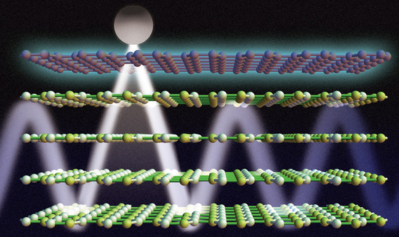
Combining light and sound to create nanoscale optical waveguides

Researchers have shown that a DC voltage applied to layers of graphene and boron nitride can be used to control light emission from a nearby atom. Here, graphene is represented by a maroon-colored top layer; boron nitride is represented by yellow-green lattices below the graphene; and the atom is represented by a grey circle. A low concentration of DC voltage (in blue) allows the light to propagate inside the boron nitride, forming a tightly confined waveguide for optical signals. (credit: Anshuman Kumar Srivastava and Jose Luis Olivares/MIT)

In a new discovery that could lead to chips that combine optical and electronic components, researchers at MIT, IBM and two universities have found a way to combine light and sound with far lower losses than when such devices are made separately and then interconnected, they say.

Light’s interaction with graphene produces vibrating electron particles called plasmons, while light interacting with hexagonal boron nitride (hBN) produces phonons (sound “particles”). Fang and his colleagues found that when the materials are combined in a certain way, the plasmons and phonons can couple, producing a strong resonance.

The properties of the graphene allow precise control over light, while hBN provides very strong confinement and guidance of the light. Combining the two makes it possible to create new “metamaterials” that marry the advantages of both, the researchers say.

The work is co-authored by MIT associate professor of mechanical engineering Nicholas Fang and graduate student Anshuman Kumar, and their co-authors at IBM’s T.J. Watson Research Center, Hong Kong Polytechnic University, and the University of Minnesota.

According to Phaedon Avouris, a researcher at IBM and co-author of the paper, “The combination of these two materials provides a unique system that allows the manipulation of optical processes.”

The two materials are structurally similar — both composed of hexagonal arrays of atoms that form two-dimensional sheets — but they each interact with light quite differently. The researchers found that these interactions can be complementary, and can couple in ways that afford a great deal of control over the behavior of light.

The hybrid material blocks light when a particular voltage is applied to the graphene layer. When a different voltage is applied, a special kind of emission and propagation, called “hyperbolicity” occurs. This phenomenon has not been seen before in optical systems, Fang says.

Nanoscale optical waveguides

The result: an extremely thin sheet of material can interact strongly with light, allowing beams to be guided, funneled, and controlled by different voltages applied to the sheet.

The combined materials create a tuned system that can be adjusted to allow light only of certain specific wavelengths or directions to propagate, they say.

These properties should make it possible, Fang says, to create tiny optical waveguides, about 20 nanometers in size —- the same size range as the smallest features that can now be produced in microchips.

“Our work paves the way for using 2-D material heterostructures for engineering new optical properties on demand,” says co-author Tony Low, a researcher at IBM and the University of Minnesota.

Single-molecule optical resolution

Another potential application, Fang says, comes from the ability to switch a light beam on and off at the material’s surface; because the material naturally works at near-infrared wavelengths, this could enable new avenues for infrared spectroscopy, he says. “It could even enable single-molecule resolution,” Fang says, of biomolecules placed on the hybrid material’s surface.

Sheng Shen, an assistant professor of mechanical engineering at Carnegie Mellon University who was not involved in this research, says, “This work represents significant progress on understanding tunable interactions of light in graphene-hBN.” The work is “pretty critical” for providing the understanding needed to develop optoelectronic or photonic devices based on graphene and hBN, he says, and “could provide direct theoretical guidance on designing such types of devices. … I am personally very excited about this novel theoretical work.”

The research team also included Kin Hung Fung of Hong Kong Polytechnic University. The work was supported by the National Science Foundation and the Air Force Office of Scientific Research.


Abstract of Tunable Light–Matter Interaction and the Role of Hyperbolicity in Graphene–hBN System

Hexagonal boron nitride (hBN) is a natural hyperbolic material, which can also accommodate highly dispersive surface phonon-polariton modes. In this paper, we examine theoretically the mid-infrared optical properties of graphene–hBN heterostructures derived from their coupled plasmon–phonon modes. We find that the graphene plasmon couples differently with the phonons of the two Reststrahlen bands, owing to their different hyperbolicity. This also leads to distinctively different interaction between an external quantum emitter and the plasmon–phonon modes in the two bands, leading to substantial modification of its spectrum. The coupling to graphene plasmons allows for additional gate tunability in the Purcell factor and narrow dips in its emission spectra.

Light-emitting, transparent flexible paper developed in China

Left: optical images of normal filter paper (bottom layer), nanocellulose-quantum dot paper (middle layer), and with acrylic resin coating added (top layer). Right: photo of luminescent nanocellulose-quantum dot paper in operation. (credit: Juan Xue et al./ACS Applied Materials & Interfaces)

The first light-emitting, transparent, flexible paper made from environmentally friendly materialshas been developed by scientists at Sichuan University in China, the scientists report in the journal ACS Applied Materials & Interfaces.

Most current flexible electronics paper designs rely on petroleum-based plastics and toxic materials.

The researchers developed a thin, clear nanocellulose paper made from wood flour and infused it with biocompatible quantum dots — tiny semiconducting crystals — made out of zinc and selenium. The paper glowed at room temperature and could be rolled and unrolled without cracking.

The researchers are currently developing papers that emit other colors than blue.

The authors acknowledge funding from the Research Fund for the Doctoral Program of Higher Education of China and the National Natural Science Foundation of China.


Abstract of Let It Shine: A Transparent and Photoluminescent Foldable Nanocellulose/Quantum Dot Paper

Exploration of environmentally friendly light-emitting devices with extremely low weight has been a trend in recent decades for modern digital technology. Herein, we describe a simple suction filtration method to develop a transparent and photoluminescent nanocellulose (NC) paper, which contains ZnSe quantum dot (QD) with high quantum yield as a functional filler. ZnSe QD can be dispersed uniformly in NC, and a quite low coefficient of thermal expansion is determined for the resultant composite paper, suggesting its good dimensional stability. These results indicate that the meeting of NC with ZnSe QD can bring a brilliant future during the information age.

Printing low-cost, flexible radio-frequency antennas with graphene ink

These scanning electron microscope images show graphene ink after it was deposited and dried (a) and then compressed (b)k, which makes the graphene nanoflakes more dense, so it improves its electrical conductivity (credit: Xianjun Huang, et al./University of Manchester)

The first low-cost, flexible, environmentally friendly radio-frequency antenna using compressed graphene ink has been printed by researchers from the University of Manchester and BGT Materials Limited. Potential uses of the new process include radio-frequency identification (RFID) tags, wireless sensors, wearable electronics, and printing on materials like paper and plastic.

Commercial RFID tags are currently made from metals like silver (very expensive) or aluminum or copper (both prone to being oxidized).

Graphene conductive ink avoids those problems and can be used to print circuits and other electronic components, but the ink contains one or more polymeric, epoxy, siloxane, and resin binders. These are required to form a continuous (unbroken) conductive film. The problem is that these binders are insulators, so they reduce the conductivity of the connection. Also, applying the binder material requires annealing, a high-heat process (similar to how soldering with a resin binder works), which would destroy materials like paper or plastic.

Printing graphene ink on paper

So the researchers developed a new process:

1. Graphene flakes are mixed with a solvent and the ink it dried and deposited on the desired surface (paper, in the case of the experiment). (This is shown in step a in the illustration above.)

2. The flakes are compressed (step b above) with a roller (similar to using a roller to compress asphalt when making a road). That step increases the graphene’s conductivity by more than 50 times.

Graphene printed on paper (credit: Xianjun Huang et al./Applied Physics Letters)

The researchers tested their compressed graphene laminate by printing a graphene antenna onto a piece of paper. The material radiated radio-frequency power effectively, said Xianjun Huang, the first author of the paper and a PhD candidate in the Microwave and Communications Group in the School of Electrical and Electronic Engineering.

The researchers plan to further develop graphene-enabled RFID tags, as well as sensors and wearable electronics. They present their results in the journal Applied Physics Letters from AIP Publishing.


Abstract of Binder-free highly conductive graphene laminate for low cost printed radio frequency applications

In this paper we demonstrate realization of printable RFID antenna by low temperature processing of graphene ink. The required ultra-low resistance is achieved by rolling compression of binder-free graphene laminate. With compression, the conductivity of graphene laminate is increased by more than 50 times compared to that of as-deposited one. Graphene laminate with conductivity of 4.3×10⁴ S/m and sheet resistance of 3.8.

Robots master skills with ‘deep learning’ technique

Robot learns to use hammer. What could go wrong? (credit: UC Berkeley)

UC Berkeley researchers have developed new algorithms that enable robots to learn motor tasks by trial and error, using a process that more closely approximates the way humans learn.

They demonstrated their technique, a type of reinforcement learning, by having a robot complete various tasks — putting a clothes hanger on a rack, assembling a toy plane, screwing a cap on a water bottle, and more — without pre-programmed details about its surroundings.

A new AI approach

“What we’re reporting on here is a new approach to empowering a robot to learn,” said Professor Pieter Abbeel of UC Berkeley’s Department of Electrical Engineering and Computer Sciences. “The key is that when a robot is faced with something new, we won’t have to reprogram it. The exact same software, which encodes how the robot can learn, was used to allow the robot to learn all the different tasks we gave it.”

The work is part of a new People and Robots Initiative at UC’s Center for Information Technology Research in the Interest of Society (CITRIS). The new multi-campus, multidisciplinary research initiative seeks to keep the advances in artificial intelligence, robotics and automation aligned to human needs.

“Most robotic applications are in controlled environments where objects are in predictable positions,” said UC Berkeley faculty member Trevor Darrell, director of the Berkeley Vision and Learning Center. “The challenge of putting robots into real-life settings, like homes or offices, is that those environments are constantly changing. The robot must be able to perceive and adapt to its surroundings.”

Neural-inspired learning

Coat-hanger training (no wire hangers!) (credit: UC Berkeley)

Conventional, but impractical, approaches to helping a robot make its way through a 3D world include pre-programming it to handle the vast range of possible scenarios or creating simulated environments within which the robot operates.

Instead, the UC Berkeley researchers turned to a new branch of artificial intelligence known as deep learning, which is loosely inspired by the neural circuitry of the human brain when it perceives and interacts with the world.

“For all our versatility, humans are not born with a repertoire of behaviors that can be deployed like a Swiss army knife, and we do not need to be programmed,” said postdoctoral researcher Sergey Levine. “Instead, we learn new skills over the course of our life from experience and from other humans. This learning process is so deeply rooted in our nervous system, that we cannot even communicate to another person precisely how the resulting skill should be executed. We can at best hope to offer pointers and guidance as they learn it on their own.”

In the world of artificial intelligence, deep learning programs create “neural nets” in which layers of artificial neurons process overlapping raw sensory data, whether it be sound waves or image pixels. This helps the robot recognize patterns and categories among the data it is receiving. People who use Siri on their iPhones, Google’s speech-to-text program or Google Street View might already have benefited from the significant advances deep learning has provided in speech and vision recognition.

Applying deep reinforcement learning to motor tasks in unstructured 3D environments has been far more challenging, however, since the task goes beyond the passive recognition of images and sounds.

BRETT masters human tasks on its own

A little nightcap? BRETT learns to put a cap on a bottle by trial and error, calculating values for 92,000 parameters. (credit: UC Berkeley)

In the experiments, the UC Berkeley researchers worked with a Willow Garage Personal Robot 2 (PR2), which they nicknamed BRETT, or Berkeley Robot for the Elimination of Tedious Tasks.

They presented BRETT with a series of motor tasks, such as placing blocks into matching openings or stacking Lego blocks. The algorithm controlling BRETT’s learning included a reward function that provided a score based upon how well the robot was doing with the task.

BRETT takes in the scene, including the position of its own arms and hands, as viewed by the camera. The algorithm provides real-time feedback via the score based upon the robot’s movements. Movements that bring the robot closer to completing the task will score higher than those that do not. The score feeds back through the neural net, so the robot can learn which movements are better for the task at hand.

This end-to-end training process underlies the robot’s ability to learn on its own. As the PR2 moves its joints and manipulates objects, the algorithm calculates good values for the 92,000 parameters of the neural net it needs to learn.

With this approach, when given the relevant coordinates for the beginning and end of the task, the PR2 could master a typical assignment in about 10 minutes. When the robot is not given the location for the objects in the scene and needs to learn vision and control together, the learning process takes about three hours.

Abbeel says the field will likely see significant improvements as the ability to process vast amounts of data improves.

“With more data, you can start learning more complex things,” he said. “We still have a long way to go before our robots can learn to clean a house or sort laundry, but our initial results indicate that these kinds of deep learning techniques can have a transformative effect in terms of enabling robots to learn complex tasks entirely from scratch. In the next five to 10 years, we may see significant advances in robot learning capabilities through this line of work.”

The latest developments will be presented on Thursday, May 28, in Seattle at the International Conference on Robotics and Automation (ICRA). The Defense Advanced Research Projects Agency, Office of Naval Research, U.S. Army Research Laboratory and National Science Foundation helped support this research.


UC Berkeley Campus Life | BRETT the robot learns to put things together on his own

Robotic arm precisely controlled by thought

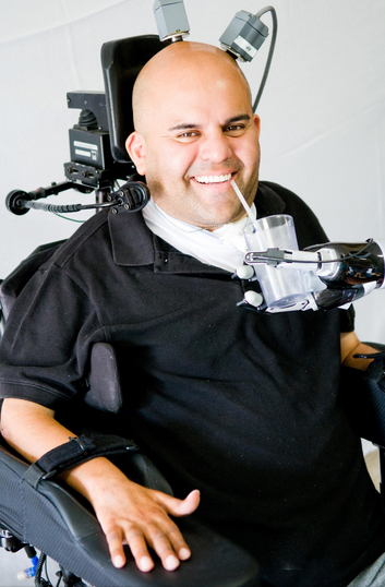
Erik Sorto smoothly controls robotic arm with his brain (credit: Spencer Kellis and Christian Klaes /Caltech)

Paralyzed from the neck down, Erik G. Sorto now can smoothly move a robotic arm just by thinking about it, thanks to a clinical collaboration between Caltech, Keck Medicine of USC and Rancho Los Amigos National Rehabilitation Center,

Previous neural prosthetic devices, such as Braingate, were implanted in the motor cortex, resulting in delayed, jerky movements. The new device was implanted in the posterior parietal cortex (PPC), a part of the brain that controls the intent to move, not the movement directly.

That makes Sorto, who has been paralyzed for over 10 years, the first quadriplegic person in the world to perform a fluid hand-shaking gesture or play “rock, paper, scissors,” using a robotic arm.

In April 2013, Keck Medicine of USC surgeons implanted a pair of small electrode arrays in two parts of the posterior parietal cortex, one that controls reach and another that controls grasp.

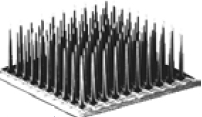
Each 4-by-4 millimeter array contains 96 active electrodes that, in turn, each record the activity of single neurons in the PPC. The arrays are connected by a cable to a system of computers that process the signals, to decode the brain’s intent and control output devices, such as a computer cursor and a robotic arm.

Although he was able to immediately move the robot arm with his thoughts, after weeks of imagining, Sorto refined his control of the arm.

Now, Sorto is able to execute advanced tasks with his mind, such as controlling a computer cursor; drinking a beverage; making a hand-shaking gesture; and performing various tasks with the robotic arm.

Designed to test the safety and effectiveness of this new approach, the clinical trial was led by principal investigator Richard Andersen, the James G. Boswell Professor of Neuroscience at Caltech, neurosurgeon Charles Y. Liu, professor of neurological surgery and neurology at the Keck School of Medicine of USC and biomedical engineering at USC, and neurologist Mindy Aisen, chief medical officer at Rancho Los Amigos.

Aisen, also a clinical professor of neurology at the Keck School of Medicine of USC, says that advancements in prosthetics like these hold promise for the future of patient rehabilitation.

NeuroPort microelectrode array implanted in Erik Sorto’s posterior parietal cortex (credit: Blackrock Microsystems)

“This research is relevant to the role of robotics and brain-machine interfaces as assistive devices, but also speaks to the ability of the brain to learn to function in new ways,” Aisen said. “We have created a unique environment that can seamlessly bring together rehabilitation, medicine, and science as exemplified in this study.”

Sorto has signed on to continue working on the project for a third year. He says the study has inspired him to continue his education and pursue a master’s degree in social work.

The results of the clinical trial appear in the May 22, 2015, edition of the journal Science. The implanted device and signal processors used in the clinical trial were the NeuroPort Array and NeuroPort Bio-potential Signal Processors developed by Blackrock Microsystems in Salt Lake City, Utah. The robotic arm used in the trial was the Modular Prosthetic Limb, developed at the Applied Physics Laboratory at Johns Hopkins.

This trial was funded by the National Institutes of Health, the Boswell Foundation, the Department of Defense, and the USC Neurorestoration Center.


Caltech | Next Generation of Neuroprosthetics: Science Explained — R. Andersen May 2015


Keck Medicine of USC | Next Generation of Neuroprosthetics: Erik’s Story


Abstract of Decoding motor imagery from the posterior parietal cortex of a tetraplegic human

Nonhuman primate and human studies have suggested that populations of neurons in the posterior parietal cortex (PPC) may represent high-level aspects of action planning that can be used to control external devices as part of a brain-machine interface. However, there is no direct neuron-recording evidence that human PPC is involved in action planning, and the suitability of these signals for neuroprosthetic control has not been tested. We recorded neural population activity with arrays of microelectrodes implanted in the PPC of a tetraplegic subject. Motor imagery could be decoded from these neural populations, including imagined goals, trajectories, and types of movement. These findings indicate that the PPC of humans represents high-level, cognitive aspects of action and that the PPC can be a rich source for cognitive control signals for neural prosthetics that assist paralyzed patients.

Tunable liquid-metal antennas

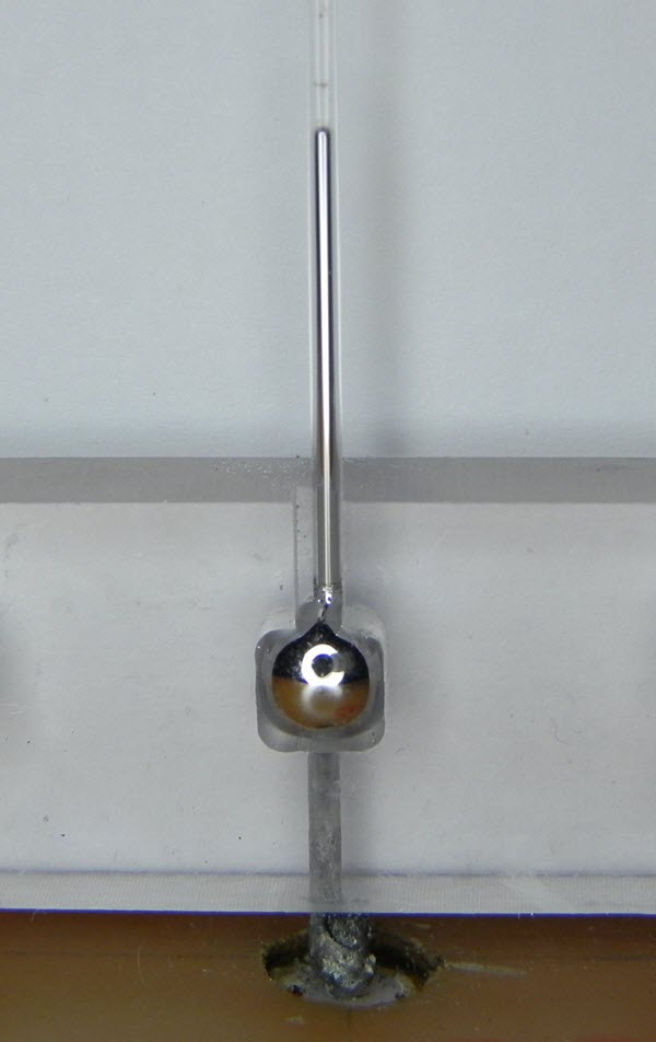
Antenna, feed, and reservoir of a liquid metal antenna (credit: Jacob Adams)

Using electrochemistry, North Carolina State University (NCSU) researchers have created a reconfigurable, voltage-controlled liquid metal antenna that may play a role in future mobile devices and the coming Internet of Things.

By placing a positive or negative electrical voltage across the interface between the liquid metal and an electrolyte, they found that they could cause the liquid metal to spread (flow into a capillary) or contract, changing its operating frequency and radiation pattern.

“Using a liquid metal — such as eutectic gallium and indium — that can change its shape allows us to modify antenna properties [such as frequency] more dramatically than is possible with a fixed conductor,” explained Jacob Adams, an assistant professor in the Department of Electrical and Computer Engineering at NCSU and a co-author of an open-access paper in the Journal of Applied Physics, from AIP Publishing.

The positive voltage “electrochemically deposits an oxide on the surface of the metal that lowers the surface tension, while a negative [voltage] removes the oxide to increase the surface tension,” Adams said. These differences in surface tension dictate which direction the metal will flow.

This advance makes it possible to “remove or regenerate enough of the ‘oxide skin’ with an applied voltage to make the liquid metal flow into or out of the capillary. We call this ‘electrochemically controlled capillarity,’ which is much like an electrochemical pump for the liquid metal,” Adams noted.

Although antenna properties can be reconfigured to some extent by using solid conductors with electronic switches, the liquid metal approach greatly increases the range over which the antenna’s operating frequency can be tuned. “Our antenna prototype using liquid metal can tune over a range of at least two times greater than systems using electronic switches,” he pointed out.

Previous liquid-metal designs typically required external pumps that can’t be easily integrated into electronic systems.

Extending frequencies for mobile devices

“Mobile device sizes are continuing to shrink and the burgeoning Internet of Things will likely create an enormous demand for small wireless systems,” Adams said. “And as the number of services that a device must be capable of supporting grows, so too will the number of frequency bands over which the antenna and RF front-end must operate. This combination will create a real antenna design challenge for mobile systems because antenna size and operating bandwidth tend to be conflicting tradeoffs.”

This is why tunable antennas are highly desirable: they can be miniaturized and adapted to correct for near-field loading problems such as the iPhone 4′s well-publicized “death grip” issue of dropped calls when by holding it by the bottom. Liquid metal systems “yield a larger range of tuning than conventional reconfigurable antennas, and the same approach can be applied to other components such as tunable filters,” Adams said.

In the long term, Adams and colleagues hope to gain greater control of the shape of the liquid metal in two-dimensional surfaces to obtain nearly any desired antenna shape. “This would enable enormous flexibility in the electromagnetic properties of the antenna and allow a single adaptive antenna to perform many functions,” he added.


Abstract of A reconfigurable liquid metal antenna driven by electrochemically controlled capillarity 

We describe a new electrochemical method for reversible, pump-free control of liquid eutectic gallium and indium (EGaIn) in a capillary. Electrochemical deposition (or removal) of a surfaceoxide on the EGaIn significantly lowers (or increases) its interfacial tension as a means to induce the liquid metal in (or out) of the capillary. A fabricated prototype demonstrates this method in a reconfigurable antenna application in which EGaIn forms the radiating element. By inducing a change in the physical length of the EGaIn, the operating frequency of the antennatunes over a large bandwidth. This purely electrochemical mechanism uses low, DC voltages to tune the antenna continuously and reversibly between 0.66 GHz and 3.4 GHz resulting in a 5:1 tuning range. Gain and radiation pattern measurements agree with electromagnetic simulations of the device, and its measured radiation efficiency varies from 41% to 70% over its tuning range.

How to make continuous rolls of graphene for volume production

Diagram of the roll-to-roll process (a) shows the arrangement of copper spools at each end of the processing tube, and how a ribbon of thin copper substrate is wound around the central tube. Cross-section view of the same setup (b) shows the gap between two tubes, where the chemical vapor deposition process occurs. Photos of the system being tested show (c) the overall system, with an arrow indicating the direction the ribbon is moving; (d) a closeup of the copper ribbon inside the apparatus, showing the holes where chemical vapor is injected; and (e) an overhead view of the copper foil passing through the system. (credit: MIT and University of Michigan researchers)

A new graphene roll-to-roll continuous manufacturing process developed by MIT and University of Michigan researchers could finally take wonder-material graphene out of the lab and into practical commercial products.

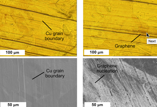
Copper substrate is shown in the process of being coated with graphene. At left, the process begins by treating the copper surface, and, at right, the graphene layer is beginning to form. Upper images are taken using visible light microscopy, and lower images using a scanning electron microscope. (credit: MIT and University of Michigan researchers)

The new process is an adaptation of a chemical vapor deposition method widely used to make graphene, using a small vacuum chamber into which a vapor containing carbon reacts on a horizontal substrate, such as a copper foil. The new system uses a similar vapor chemistry, but the chamber is in the form of two concentric tubes, one inside the other, and the substrate is a thin ribbon of copper that slides smoothly over the inner tube.

Gases flow into the tubes and are released through precisely placed holes, allowing for the substrate to be exposed to two mixtures of gases sequentially. The first region is called an annealing region, used to prepare the surface of the substrate; the second region is the growth zone, where the graphene is formed on the ribbon. The chamber is heated to approximately 1,000 degrees Celsius to perform the reaction.

The researchers have designed and built a lab-scale version of the system, and found that when the ribbon is moved through at a rate of 25 millimeters (1 inch) per minute, a very uniform, high-quality single layer of graphene is created. When rolled 20 times faster, it still produces a coating, but the graphene is of lower quality, with more defects.

A “big leap”

Graphene is a material with a host of potential applications, including use in solar panels that could be integrated into windows, and membranes to desalinate and purify water. But all these possible uses face the same big hurdle: the need for a scalable and cost-effective method for continuous manufacturing of graphene films.

For these practical uses, “You’re going to need to make acres of it, repeatedly and in a cost-effective manner,” says MIT mechanical engineering Associate Professor A. John Hart, senior author of the open-access Scientific Reports paper.

Making such quantities of graphene would represent a big leap from present approaches, where researchers struggle to produce small quantities of graphene — often laboriously pulling these sheets from a lump of graphite using adhesive tape, or producing a film the size of a postage stamp using a laboratory furnace.

The new method promises to enable continuous production, using a thin metal foil as a substrate, in an industrial process where the material would be deposited onto the foil as it smoothly moves from one spool to another. The resulting sheets would be limited in size only by the width of the rolls of foil and the size of the chamber where the deposition would take place.

Applications

Because a continuous process eliminates the need to stop and start to load and unload materials from a fixed vacuum chamber, as in today’s processing methods, it could lead to significant scale-up of production. That could finally unleash applications for graphene, which has unique electronic and optical properties and is one of the strongest materials known.

Some potential applications, such as filtration membranes, may require very high-quality graphene, but other applications, such as thin-film heaters may work well enough with lower-quality sheets, says Hart, who is the Mitsui Career Development Associate Professor in Contemporary Technology at MIT.

So far, the new system produces graphene that is “not quite [equal to] the best that can be done by batch processing,” Hart says — but “to our knowledge, it’s still at least as good” as what’s been produced by other continuous processes. Further work on details such as pretreatment of the substrate to remove unwanted surface defects could lead to improvements in the quality of the resulting graphene sheets, he says.

The team is studying these details, Hart adds, and learning about tradeoffs that can inform the selection of process conditions for specific applications, such as between higher production rate and graphene quality. Then, he says, “The next step is to understand how to push the limits, to get it 10 times faster or more.”

Hart says that while this study focuses on graphene, the machine could be adapted to continuously manufacture other two-dimensional materials, or even to growing arrays of carbon nanotubes, which his group is also studying.

“This is high-quality research that represents significant progress on the path to scalable production methods for large-area graphene,” says Charlie Johnson, a professor of physics and astronomy at the University of Pennsylvania who was not involved in this work. “I think that the concentric tube approach is very creative. It has the potential to lead to significantly lower production costs for graphene, if it can be scaled to larger copper-foil widths.”

The work was supported by the National Science Foundation and the Air Force Office of Scientific Research.

New technology could fundamentally improve future wireless communications

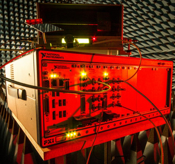
Novel full-duplex transceiver (top device) in an anechoic chamber for testing (credit: Sam Duckerin)

A new electronics technique that could allow a radio device to transmit and receive on the same channel at the same time (“full duplex,” or simultaneous, two-way transmission) has been developed by researchers at the University of Bristol’s Communication Systems and Networks research group. The technique can estimate and cancel out the interference from a device’s own transmission.

Today’s cell phones and other communication devices use twice as much of the radio spectrum as necessary. The new system requires only one channel (set of frequencies) for two-way communication,so it uses only half as much spectrum compared to current technology.

The new technology combines electrical balance isolation and active radio frequency cancellation. Their prototype can suppress interference by a factor of more than 100 million and uses low-cost, small-form-factor technologies, making it well suited to use in mobile devices such as smartphones.

Significant impacts on mobile and WiFi systems

For future cellular systems (such as 5G systems), the new technology would deliver increased capacity and data rates, or alternatively, the network operators could provide the same total network capacity with fewer base-station sites, reducing the cost and environmental impact of running the network.

In today’s mobile devices, a separate filtering component is required for each frequency band, and because of this, today’s mobiles phone do not support all of the frequency channels available internationally. Different devices are manufactured for different regions of the world, so there are currently no 4G phones capable of unrestricted global roaming.

In Wi-Fi systems, the new design would double the capacity of a Wi-Fi access point, allowing for more simultaneous users or higher data rates.

Replacing these filters with the research team’s duplexer circuit would create smaller and cheaper devices, and would allow manufacturers to produce a single model for the entire world. This would enable global roaming on 4G and would further decrease cost through greater economies of scale.

The team had published papers about their research in the IEEE Journal on Selected Areas in Communications special issue on full duplex radio, and in this month’s issue of the IEEE Communications Magazine and has filed patents.


Abstract of Electrical balance duplexing for small form factor realization of in-band full duplex

Transceiver architectures utilizing various self-interference suppression techniques have enabled simultaneous transmission and reception at the same frequency. This full-duplex wireless offers the potential for a doubling of spectral efficiency; however, the requirement for high transmit-to-receive isolation presents formidable challenges for the designers of full duplex transceivers. Electrical balance in hybrid junctions has been shown to provide high transmit- to-receive isolation over significant bandwidths. Electrical balance duplexers require just one antenna, and can be implemented on-chip, making this an attractive technology for small form factor devices. However, the transmit-toreceive isolation is sensitive to antenna impedance variation in both the frequency domain and time domain, limiting the isolation bandwidth and requiring dynamic adaptation. Various contributions concerning the implementation and performance of electrical balance duplexers are reviewed and compared, and novel measurements and simulations are presented. Results demonstrate the degradation in duplexer isolation due to imperfect system adaptation in user interaction scenarios, and requirements for the duplexer adaptation system are discussed.


Abstract of Optimum Single Antenna Full Duplex Using Hybrid Junctions

This paper investigates electrical balance (EB) in hybrid junctions as a method of achieving transmitter-receiver isolation in single antenna full duplex wireless systems. A novel technique for maximizing isolation in EB duplexers is presented, and we show that the maximum achievable isolation is proportional to the variance of the antenna reflection coefficient with respect to frequency. Consequently, antenna characteristics can have a significant detrimental impact on the isolation bandwidth. Simulations that include embedded antenna measurements show a mean isolation of 62 dB over a 20-MHz bandwidth at 1.9 GHz but relatively poor performance at wider bandwidths. Furthermore, the operational environment can have a significant impact on isolation performance. We present a novel method of characterizing radio reflections being returned to a single antenna. Results show as little as 39 dB of attenuation in the radio echo for a highly reflective indoor environment at 1.9 GHz and that the mean isolation of an EB duplexer is reduced by 7 dB in this environment. A full duplex architecture exploiting EB is proposed.

NASA new CubeSat concept for planetary exploration

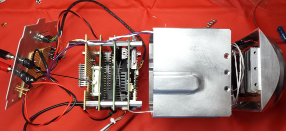
Technologist Jaime Esper and his team are planning to test the stability of a prototype entry vehicle — the Micro-Reentry Capsule (MIRCA) — this summer during a high-altitude balloon mission from Ft. Sumner, New Mexico (credits: NASA/Goddard)

Jaime Esper, a technologist at NASA’s Goddard Space Flight Center has developed a CubeSat concept that would allow scientists to use less-expensive cubesat (tiny-satellite) technology to observe physical phenomena beyond the current low-Earth-orbit limit.

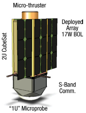
The CubeSat Application for Planetary Entry Missions (CAPE) concept involves a service module that would propel the spacecraft to its  target and a separate planetary entry probe that could survive a rapid dive through the atmosphere of an extraterrestrial planet, all while reliably transmitting scientific and engineering data.

CAPE in its deployed configuration (credit: Jaime Esper/NASA Goddard)

Planetary landings

Esper and his team are planning to test the stability of a prototype entry vehicle, the Micro-Reentry Capsule (MIRCA), this summer during a high-altitude balloon mission from Fort Sumner, New Mexico.

The CAPE/MIRCA spacecraft, including the service module and entry probe, would weigh less than 11 pounds (4.9 kilograms) and measure no more than 4 inches (10.1 centimeters) on a side. After being ejected from a canister housed by its mother ship, the tiny spacecraft would unfurl its miniaturized solar panels or operate on internal battery power to begin its journey to another planetary body.

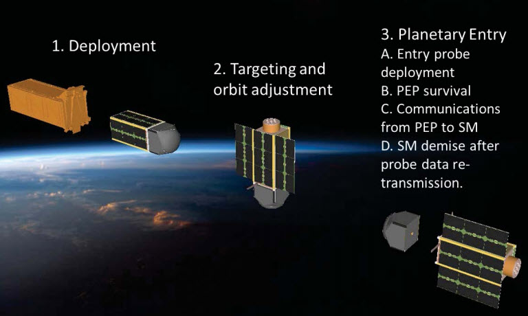
Once it reached its destination, the sensor-loaded entry vehicle would separate from its service module and begin its descent through the target’s atmosphere. It would communicate atmospheric pressure, temperature, and composition data to the mother ship, which then would transmit the information back to Earth.

The beauty of CubeSats is their versatility. Because they are relatively inexpensive to build and deploy, scientists could conceivably launch multiple spacecraft for multi-point sampling — a capability currently not available with single planetary probes that are the NASA norm today. Esper would equip the MIRCA craft with accelerometers, gyros, thermal and pressure sensors, and radiometers, which measure specific gases; however, scientists could tailor the instrument package depending on the targets, Esper said.

A generic CAPE operations concept, from system deployment to probe release and entry into a given planetary atmosphere. Three mission phases are identified: 1. Deployment, 2. Targeting, and 3. Planetary Entry. (credit: Jaime Esper/NASA Goddard)