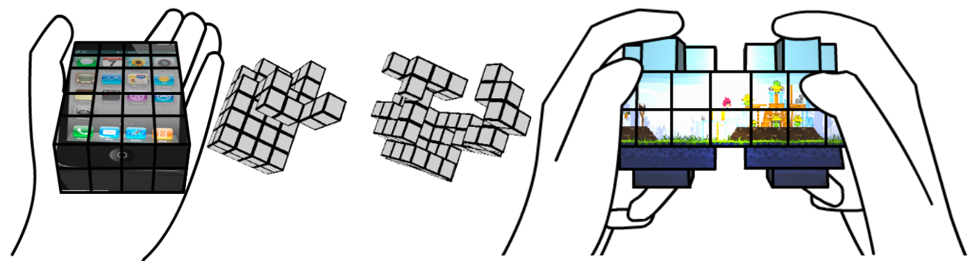
Cubimorph is an interactive device made of a chain of reconfigurable modules that shape-shifts into any shape that can be made out of a chain of cubes, such as transforming from a mobile phone to a game console. (credit: Anne Roudaut et al./Proceedings of the ICRA 2016)
British researchers and Google have independently developed revolutionary concepts for Lego-like modular interactive mobile devices.
The British team’s design, called Cubimorph, is constructed of a chain of cubes. It has touchscreens on each of the six module faces and uses a hinge-mounted turntable mechanism to self-reconfigure in the user’s hand. One example: a mobile phone that can transform into a console when a user launches a game.
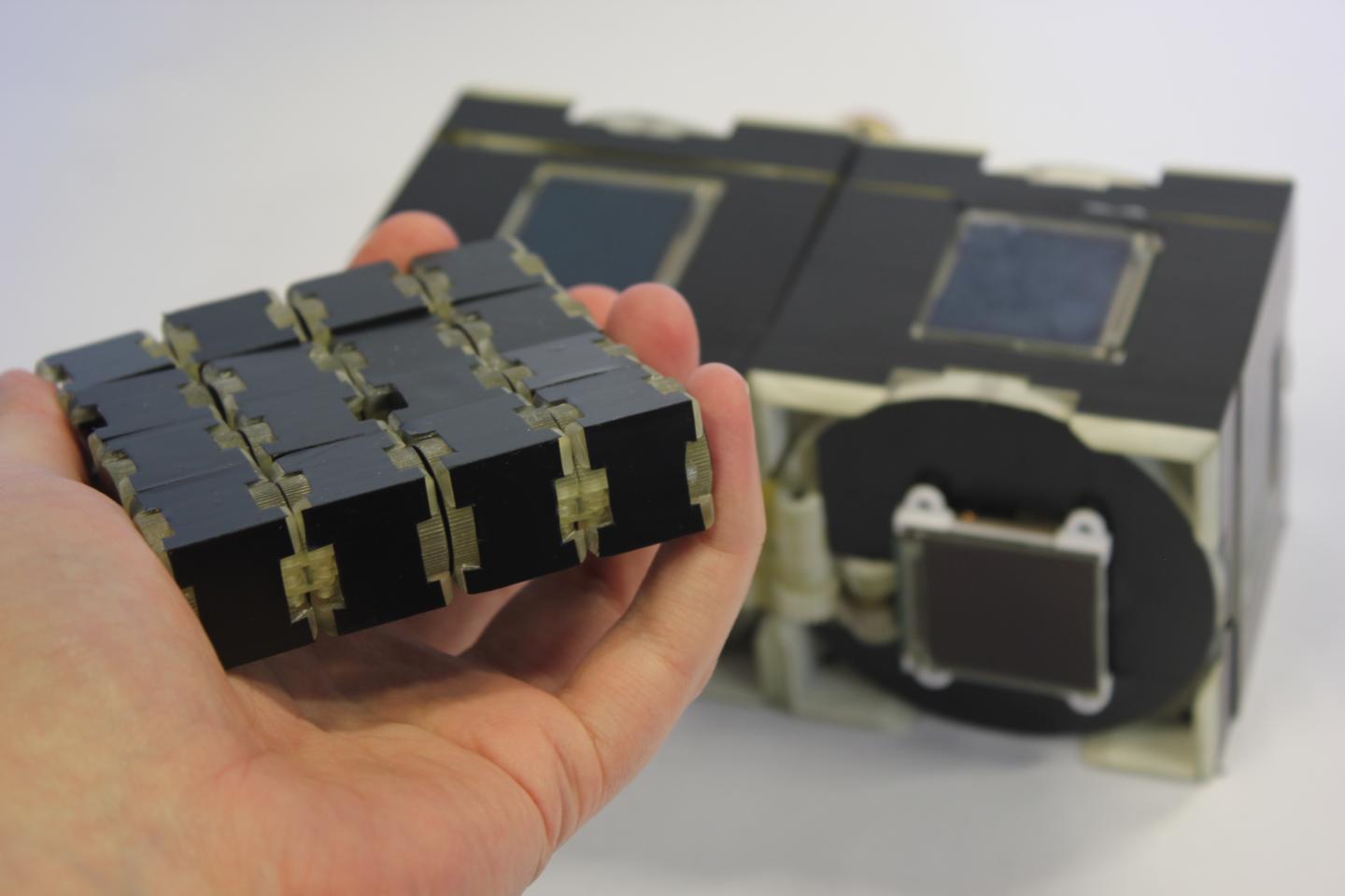
Proof-of-concept prototype of Cubimorph (credit: BIG/University of Bristol)
The research team has developed three prototypes demonstrating key aspects — turntable hinges, embedded touchscreens, and miniaturization.
BIG | Cubimorph: Designing Modular Interactive Devices
The modular interactive design is a step toward the vision of programmable matter, where interactive devices change their shape to meet specific user needs.
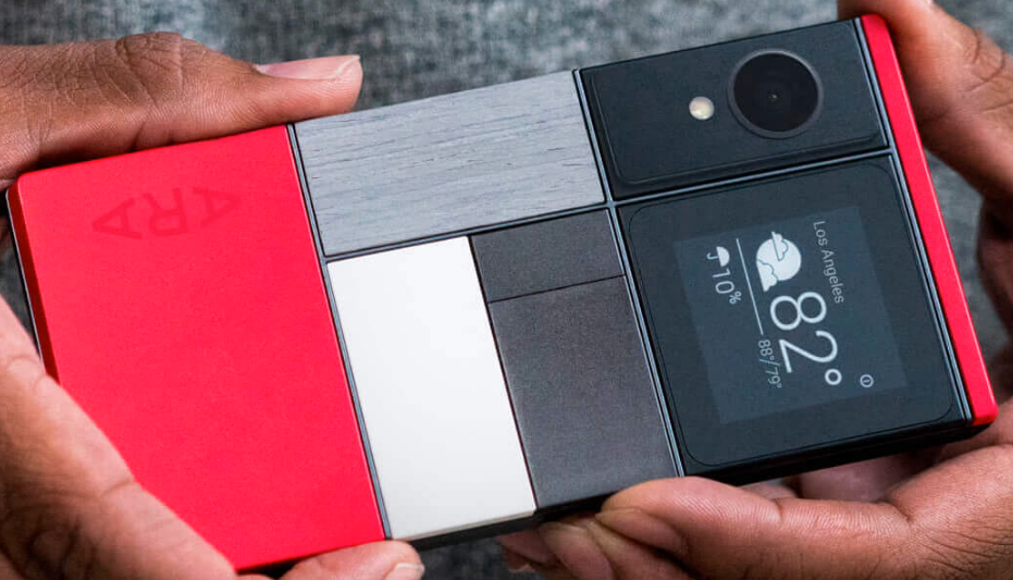
Ara, launched at Google’s I/O developer conference, uses a frame that contains all the functionality of a smartphone (CPU, GPU, antennas, sensors, battery, and display) plus six flexible slots for easy swapping of modules. “Slide any Ara module into any slot and it just works,” is the concept. Powering this is Greybus, a new bit of software deep in the Android stack that supports instantaneous connections, power efficiency, and data-transfer rates of up to 11.9 Gbps. The Developer Edition will ship in Fall 2016, with a consumer version in 2017.
Google | Ara: What’s next
Abstract of Cubimorph: Designing Modular Interactive Devices
We introduce Cubimorph, a modular interactive device that accommodates touchscreens on each of the six module faces, and that uses a hinge-mounted turntable mechanism to self-reconfigure in the user’s hand. Cubimorph contributes toward the vision of programmable matter where interactive devices reconfigure in any shape that can be made out of a chain of cubes in order to fit a myriad of functionalities, e.g. a mobile phone shifting into a console when a user launches a game. We present a design rationale that exposes user requirements to consider when designing homogeneous modular interactive devices. We present our Cubimorph mechanical design, three prototypes demonstrating key aspects (turntable hinges, embedded touchscreens and miniaturization), and an adaptation of the probabilistic roadmap algorithm for the reconfiguration.
Virtual environments for training a robot dog (credit: Washington State University)
Researchers at Washington State University are using ideas from animal training to help non-expert users teach robots how to do desired tasks.
As robots become more pervasive in society, humans will want them to do chores like cleaning house or cooking. But to get a robot started on a task, people who aren’t computer programmers will have to give it instructions. “So we needed to provide a way for everyone to train robots, without programming,” said Matthew Taylor, Allred Distinguished Professor in the WSU School of Electrical Engineering and Computer Science.
User feedback improves robot performance
With Bei Peng, a doctoral student in computer science, and collaborators at Brown University and North Carolina State University, Taylor designed a computer program that lets humans without programming expertise teach a virtual robot that resembles a dog in WSU’s Intelligent Robot Learning Laboratory.
For the study, the researchers varied the speed at which their virtual dog reacted. As when somebody is teaching a new skill to a real animal, the slower movements let the trainer know that the virtual dog was unsure of how to behave, so trainers could provide clearer guidance to help the robot learn better.
The researchers have begun working with physical robots as well as virtual ones. They also hope to eventually also use the program to help people learn to be more effective animal trainers.
The researchers recently presented their work at the international Autonomous Agents and Multiagent Systems conference, a scientific gathering for agents and robotics research. Funding for the project came from a National Science Foundation grant.
Bei Peng/WSU | Dog Training — AAMAS 2016
Abstract of A Need for Speed: Adapting Agent Action Speed to Improve Task Learning from Non-Expert Humans
As robots become pervasive in human environments, it is important to enable users to effectively convey new skills without programming. Most existing work on Interactive Reinforcement Learning focuses on interpreting and incorporating non-expert human feedback to speed up learning; we aim to design a better representation of the learning agent that is able to elicit more natural and effective communication between the human trainer and the learner, while treating human feedback as discrete communication that depends probabilistically on the trainer’s target policy. This work entails a user study where participants train a virtual agent to accomplish tasks by giving reward and/or punishment in a variety of simulated environments. We present results from 60 participants to show how a learner can ground natural language commands and adapt its action execution speed to learn more efficiently from human trainers. The agent’s action execution speed can be successfully modulated to encourage more explicit feedback from a human trainer in areas of the state space where there is high uncertainty. Our results show that our novel adaptive speed agent dominates different fixed speed agents on several measures of performance. Additionally, we investigate the impact of instructions on user performance and user preference in training conditions.
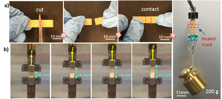
Penn State researchers have developed a flexible electronic material that self-heals to restore multiple functions, even after repeated breaks. (Top row) The material is cut in half, then reattached. After healing for 30 minutes, the material is still able to be stretched and hold weight. (credit: Qing Wang, Penn State)
A new electronic material created by an international team headed by Penn State scientists can heal all its functions automatically, even after breaking multiple times. The new material could improve the durability of wearable electronics.
Electronic materials have been a major stumbling block for the advance of flexible electronics because existing materials do not function well after breaking and healing.
“Wearable and bendable electronics are subject to mechanical deformation over time, which could destroy or break them,” said Qing Wang, professor of materials science and engineering, Penn State. “We wanted to find an electronic material that would repair itself to restore all of its functionality, and do so after multiple breaks.”
In the past, researchers have been able to create self-healable materials (such as these, covered on KurzweilAI) that can restore a single function after breaking. But restoring a suite of functions is critical for creating effective wearable electronics. For example, if a dielectric material retains its electrical resistivity after self-healing but not its thermal conductivity, that could put electronics at risk of overheating.
The material that Wang and his team created restores all properties needed for use as a dielectric in wearable electronics — mechanical strength, breakdown strength to protect against surges, electrical resistivity, thermal conductivity, and dielectric (insulating) properties. They published their findings online in Advanced Functional Materials.
“Most research into self-healable electronic materials has focused on electrical conductivity but dielectrics have been overlooked,” said Wang. “We need conducting elements in circuits but we also need insulation and protection for microelectronics.” Most self-healable materials are also soft or “gum-like,” said Wang, but the material he and his colleagues created is very tough in comparison.
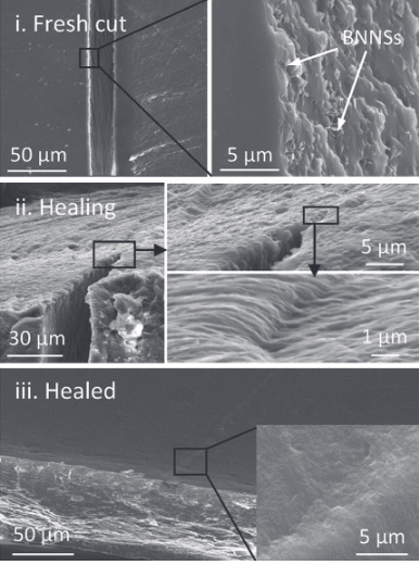
SEM images of healing process of polymer nanocomposite with 8% volume boron nitride nanosheets: (i) freshly cut, (ii) healing in 15 min, and (iii) completely healed in 30 min (credit: Lixin Xing et al./Advanced Functional Materials)
His team added boron nitride nanosheets to a base material of plastic polymer. The material is able to self-heal because boron nitride nanosheets connect to one another with hydrogen bonding groups functionalized onto their surface. When two pieces are placed in close proximity, the electrostatic attraction naturally occurring between both bonding elements draws them close together. When the hydrogen bond is restored, the two pieces are “healed.”
Depending on the percentage of boron nitride nanosheets added to the polymer, this self-healing may require additional heat or pressure, but some forms of the new material can self-heal at room temperature when placed next to each other.
Unlike other healable materials that use hydrogen bonds, boron nitride nanosheets are impermeable to moisture. This means that devices using this dielectric material can operate effectively within high humidity contexts such as in a shower or at a beach.
“This is the first time that a self-healable material has been created that can restore multiple properties over multiple breaks, and we see this being useful across many applications,” said Wang.
Harbin Institute of Technology researches also collaborated on this research, which was supported by the China Scholarship Council.
Penn State Research Communications | Flexible Insulator
Abstract of Self-Healable Polymer Nanocomposites Capable of Simultaneously Recovering Multiple Functionalities
The continuous evolution toward electronics with high power densities and integrated circuits with smaller feature sizes and faster speeds places high demands on a set of material properties, namely, the electrical, thermal, and mechanical properties of polymer dielectrics. Herein, a supramolecular approach is described to self-healable polymer nanocomposites that are mechanically robust and capable of restoring simultaneously structural, electrical, dielectric, and thermal transport properties after multiple fractures. With the incorporation of surface-functionalized boron nitride nanosheets, the polymer nanocomposites exhibit many desirable features as dielectric materials such as higher breakdown strength, larger electrical resistivity, improved thermal conductivity, greater mechanical strength, and much stabilized dielectric properties when compared to the pristine polymer. It is found that the recovery condition has remained the same during sequential cycles of cutting and healing, therefore suggesting no aging of the polymer nanocomposites with mechanical breakdown. Moreover, moisture has a minimal effect on the healing and dielectric properties of the polymer nanocomposites, which is in stark contrast to what is typically observed in the hydrogen-bonded supramolecular structures.
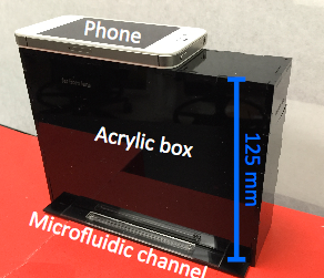
Stanford University School of Engineering | This easy-to-assemble black box is part of an experimental urinalysis testing system designed by Stanford engineers. The black box is meant to enable a smartphone camera to capture video that accurately analyzes color changes in a standard paper dipstick to detect conditions of medical interest.
Two Stanford University electrical engineers have designed a simple new low-cost, portable urinalysis device that could allow patients to get consistently accurate urine test results at home.
The system uses a black box and smartphone camera to analyze a standard color-changing paper test, using a medical dipstick dipped into the urine specimen, to measure levels of glucose, blood, protein, and other chemicals — which can indicate evidence of kidney disease, diabetes, urinary tract infections and even signs of bladder cancer.
The current standard dipstick test uses a paper strip with 10 square pads. Dipped in a sample, each pad changes color to screen for the presence of a different disease-indicating chemical. After waiting the appropriate amount of time, a medical professional — or, increasingly, an automated system — compares the pad shades to a color reference chart for results.
But the test takes time, costs money, and creates backlogs for clinics and primary care physicians. The results are often inconclusive, requiring both patient and doctor to book another appointment. So patients with long-term conditions like chronic urinary tract infections must wait for results to confirm what both patient and doctor already know before getting antibiotics. Tracking patients’ progress with multiple urine tests a day is out of the question.
Some innovators have tried to create simple, do-it-yourself systems, but they can be error-prone, said Audrey (Ellerbee) Bowden, assistant professor of electrical engineering at Stanford. “You think it’s easy — you just dip the stick in urine and look for the color change, but there are things that can go wrong,” she said. “Doctors don’t end up trusting those results as accurate.”
A simplified home urinanalysis system
Prototype urinalysis device (credit: Gennifer T. Smith et al./Lab on a Chip)
Writing in Lab on a Chip, a journal of the Royal Society of Chemistry, Bowden and Gennifer Smith, a PhD student in electrical engineering, explain they designed their system to overcome three main potential errors in a home test: inconsistent lighting, urine volume control, and timing.
To fix this, the engineers designed a multi-layered system to load urine onto the dipstick. A dropper squeezes urine into a hole in the first layer, filling up a channel in the second layer, and ten square holes in the third layer. Some clever engineering ensures that a uniform volume of urine is deposited on each of the ten pads on the dipstick at just the right time.
Finally, a smartphone is placed on top of the black box with the video camera focused on the dipstick inside the box. Custom software reads video from the smartphone and controls the timing and color analysis.
To perform the test a person would load the urine and then push the third layer into the box. When the third layer hits the back of the box, it signals the phone to begin the video recording at the precise moment when the urine is deposited on the pads.
Timing is critical to the analysis. Pads have readout times ranging from 30 seconds to 2 minutes. Once the two minutes are up, the person can transfer the recording to a software program on their computer. For each pad, it pulls out the frames from the correct time and reads out the results.
The engineers also plan to design an app to send the results directly to the doctor.
Funding for this research came from the National Institutes of Health, the Rose Hills Foundation Graduate Engineering Fellowship, the Electrical Engineering Department New Projects Graduate Fellowship, the Oswald G. Villard Jr. Engineering Fellowship, the Stanford Graduate Fellowship and the National Science Foundation Graduate Research Fellowship.
Abstract of Robust dipstick urinalysis using a low-cost, micro-volume slipping manifold and mobile phone platform
We introduce a novel manifold and companion software for dipstick urinalysis that eliminate many of the aspects that are traditionally plagued by user error: precise sample delivery, accurate readout timing, and controlled lighting conditions. The proposed all-acrylic slipping manifold is reusable, reliable, and low in cost. A simple timing mechanism ensures results are read out at the appropriate time. Results are obtained by capturing videos using a mobile phone and by analyzing them using custom-designed software. We show that the results obtained with the proposed device are as accurate and consistent as a properly executed dip-and-wipe method, the industry gold-standard, suggesting the potential for this strategy to enable confident urinalysis testing in home environments.
An “origami robot” unfolds itself from an ingestible capsule. It could be used by a physician to perform a remote-controlled operation (credit: Melanie Gonick/MIT)
MIT researchers and associates have developed a tiny “origami robot” that can unfold itself from a swallowed capsule and, steered by a physician via an external magnetic field, crawl across the stomach wall to operate on a patient. For example, it can remove a swallowed button battery or patch a wound.
System for remote-controlled clinical procedures via origami-based robot. A patient swallows an iced capsule, which melts when it reaches the stomach, releasing the robot from a folded origami structure. To remove a foreign body (such as a button battery), the physician controls the robot from outside the body via a magnetic field that affects the magnet inside the delivery structure, allowing the robot to push the foreign body into the GI system. The robot can also treat an inflammation by releasing a drug contained in the delivery structure. (credit: Shuhei Miyashita et al./ICRA Proceedings)
Every year, 3,500 swallowed button batteries are reported in the U.S. alone. Frequently, the batteries are digested normally, but if they come into prolonged contact with the tissue of the esophagus or stomach, they can cause an electric current that produces hydroxide, which burns the tissue.
The researchers at MIT, the University of Sheffield, and the Tokyo Institute of Technology presented the work last week at the International Conference on Robotics and Automation. The design built on previous work (see related links below) from the research group of Daniela Rus, the Andrew and Erna Viterbi Professor in MIT’s Department of Electrical Engineering and Computer Science. The new robot is a successor to one reported at this conference last year, with an improved design, tested in a pig stomach.
Rus and the team plan further developments, including the robot’s ability to perform procedures without physician remote control.
MIT | Ingestible origami robot
Abstract of Ingestible, Controllable, and Degradable Origami Robot for Patching Stomach Wounds
Developing miniature robots that can carry out versatile clinical procedures inside the body under the remote instructions of medical professionals has been a long time challenge. In this paper, we present origami-based robots that can be ingested into the stomach, locomote to a desired location, remove a foreign body, deliver drugs, and biodegrade. We designed and fabricated composite material sheets for a biocompatible and biodegradable robot that can be encapsulated in ice for delivery through the esophagus, embed a drug layer that is passively released to a wounded area, and be remotely controlled to carry out underwater maneuvers specific to the tasks using magnetic fields. The performances of the robots are demonstrated in a simulated physical environment consisting of an esophagus and stomach with properties similar to the biological organs.
For the first time, scientists at IBM Research have demonstrated reliably storing 3 bits of data per cell using a relatively new memory technology known as phase-change memory (PCM). In this photo, the experimental multi-bit PCM chip used by IBM scientists is connected to a standard integrated circuit board. The chip consists of a 2 × 2 Mcell array with a 4- bank interleaved architecture. The memory array size is 2 × 1000 μm × 800 μm. The PCM cells are based on doped-chalcogenide alloy and were integrated into the prototype chip, serving as a characterization vehicle in 90 nm CMOS baseline technology. (credit: IBM Research)
Scientists at IBM Research have demonstrated — for the first time (today, May 17), at the IEEE International Memory Workshop in Paris — reliably storing 3 bits of data per cell in a 64k-cell array in a memory chip*, using a relatively new memory technology known as phase-change memory (PCM). Previously, scientists at IBM and elsewhere successfully demonstrated the ability to store only 1 bit per cell in PCM.
The current memory landscape includes DRAM, hard disk drives, and flash. But in the last several years, PCM has attracted the industry’s attention as a potential universal memory technology based on its combination of read/write speed, endurance, non-volatility and density. For example, PCM doesn’t lose data when powered off, unlike DRAM, and the technology can endure at least 10 million write cycles, compared to an average flash USB stick, which tops out at 3,000 write cycles.
IBM suggests this research breakthrough provides fast and easy storage to capture the exponential growth of data from mobile devices and the Internet of Things.
Scientists have long been searching for a universal, non-volatile memory technology with performance far superior to flash — today’s most ubiquitous non-volatile memory technology. The benefits of such a memory technology would allow computers and servers to boot instantaneously and would significantly enhance the overall performance of IT systems. A promising contender is PCM, which can write and retrieve data 100 times faster than Flash and enable high storage capacities, and like flash, not lose data when the power is turned off. Unlike flash, PCM is also very durable and can endure at least 10 million write cycles, compared to current enterprise-class flash at 30,000 cycles or consumer-class flash at 3,000 cycles. While 3,000 cycles will outlive many consumer devices, 30,000 cycles are orders of magnitude too low to be suitable for enterprise applications. (credit: IBM Research)
IBM scientists envision standalone PCM as well as hybrid applications that combine PCM and flash storage, with PCM as an extremely fast cache. For example, a mobile phone’s operating system could be stored in PCM, enabling the phone to launch in a few seconds. In the enterprise space, entire databases could be stored in PCM for blazing fast query processing in time-critical online applications, such as financial transactions.
Machine learning algorithms using large datasets will also see a speed boost by reducing the latency overhead when reading the data between iterations.
How PCM Works: answering the grand challenge of combining properties of DRAM and flash
PCM materials exhibit two stable states: the amorphous (without a clearly defined structure) and crystalline (with structure) phases (low and high electrical conductivity, respectively).
To store a “0″ or a “1″ bit on a PCM cell, a high or medium electrical current is applied to the material. A “0″ can be programmed to be written in the amorphous phase and a “1″ in the crystalline phase, or vice versa. Then to read the bit back, a low voltage is applied. This is how re-writable (but slower) Blu-ray discs** store videos.
Phase-change memory (PCM) is one of the most promising candidates for next-generation non-volatile memory technology. The cross-sectional tunneling electron microscopy (TEM) image of a mushroom-type PCM cell is shown in this photo. The cell consists of a layer of phase-change material, such as germanium antimony telluride (GST), sandwiched between a bottom and a top electrode. In this architecture, the bottom electrode has a radius (denoted as rE ) of approx. 15 nm and is fabricated by sub-lithographic means. The top electrode has a radius in excess of 100 nm and the thickness of the phase change layer is approx. 100 nm. A transistor or a diode is typically employed as the access device. (credit: IBM Research — Zurich)
“Phase change memory is the first instantiation of a universal memory with properties of both DRAM and flash, thus answering one of the grand challenges of our industry,” said Haris Pozidis, PhD., an author of the workshop paper and the manager of non-volatile memory research at IBM Research–Zurich. “Reaching 3 bits per cell is a significant milestone because at this density, the cost of PCM will be significantly less than DRAM and closer to flash.”
To achieve multi-bit storage, IBM scientists have developed two innovative enabling technologies: a set of drift-immune cell-state metrics and drift-tolerant coding and detection schemes***. “Combined, these advancements address the key challenges of multi-bit PCM, including drift, variability, temperature sensitivity, and endurance cycling,” said IBM Fellow Evangelos Eleftheriou, PhD.
IBM scientists have also demonstrated, for the first time, phase-change memory attached to POWER8-based servers.
* At elevated temperatures and after 1 million endurance cycles.
*** More specifically, the new cell-state metrics measure a physical property of the PCM cell that remains stable over time, and are thus insensitive to drift, which affects the stability of the cell’s electrical conductivity with time. To provide additional robustness of the stored data in a cell over ambient temperature fluctuations, a novel coding and detection scheme is employed. This scheme adaptively modifies the level thresholds that are used to detect the cell’s stored data so that they follow variations due to temperature change. As a result, the cell state can be read reliably over long time periods after the memory is programmed, thus offering non-volatility.
The experimental multi-bit PCM chip used by IBM scientists is connected to a standard integrated circuit board. The chip consists of a 2 × 2 Mcell array with a four-bank interleaved architecture. The memory array size is 2 × 1000 μm × 800 μm. The PCM cells are based on doped-chalcogenide alloy and were integrated into the prototype chip serving as a characterization vehicle in 90 nm CMOS baseline technology.
IBM Research | IBM Scientists Achieve Storage Memory Breakthrough
Abstract of Multilevel-Cell Phase Change Memory: A Viable Technology
In order for any non-volatile memory (NVM) to be considered a viable technology, its reliability should be verified at the array level. In particular, properties such as high endurance and at least moderate data retention are considered essential. Phase-change memory (PCM) is one such NVM technology that possesses highly desirable features and has reached an advanced level of maturity through intensive research and development in the past decade. Multilevel-cell (MLC) capability, i.e., storage of two bits per cell or more, is not only desirable as it reduces the effective cost per storage capacity, but a necessary feature for the competitiveness of PCM against the incumbent technologies, namely DRAM and Flash memory. MLC storage in PCM, however, is seriously challenged by phenomena such as cell variability, intrinsic noise, and resistance drift. We present a collection of advanced circuit-level solutions to the above challenges, and demonstrate the viability of MLC PCM at the array level. Notably, we demonstrate reliable storage and moderate data retention of 2 bits/cell PCM, on a 64 k cell array, at elevated temperatures and after 1 million SET/RESET endurance cycles. Under similar operating conditions, we also show feasibility of 3 bits/cell PCM, for the first time ever.
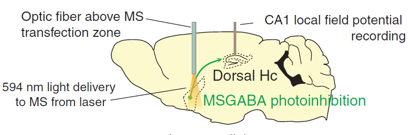
Inhibition of media septum GABA neurons during rapid eye movement (REM) sleep reduces theta rhythm (a characteristic of REM sleep). Schematic of the in vivo recording configuration: an optic fiber delivered orange laser light to the media septum part of the brain, allowing for optogenetic inhibition of media septum GABA neurons while recording the local field potential signal from electrodes implanted in hippocampus area CA1. (credit: Richard Boyce et al./Science)
A study published in the journal Science by researchers at the Douglas Mental Health University Institute at McGill University and the University of Bern provides the first evidence that rapid eye movement (REM) sleep — the phase where dreams appear — is directly involved in memory formation (at least in mice).
“We already knew that newly acquired information is stored into different types of memories, spatial or emotional, before being consolidated or integrated,” says Sylvain Williams, a researcher and professor of psychiatry at McGill*. “How the brain performs this process has remained unclear until now. We were able to prove for the first time that REM sleep (dreaming) is indeed critical for normal spatial memory formation in mice,” said Williams.
Dream quest
Hundreds of previous studies have tried unsuccessfully to isolate neural activity during REM sleep using traditional experimental methods. In this new study, the researchers instead used optogenetics, which enables scientists to precisely target a population of neurons and control its activity by light.
“We chose to target [GABA neurons in the media septum] that regulate the activity of the hippocampus, a structure that is critical for memory formation during wakefulness and is known as the ‘GPS system’ of the brain,” Williams says.
To test the long-term spatial memory of mice, the scientists trained the rodents to spot a new object placed in a controlled environment where two objects of similar shape and volume stand. Spontaneously, mice spend more time exploring a novel object than a familiar one, showing their use of learning and recall.
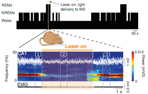
Shining orange laser light on media septum (MS) GABA neurons during REM sleep reduces frequency and power (purple section) of neuron signals in dorsal CA1 area of hippocampus (credit: Richard Boyce et al./Science)
When these mice were in REM sleep, however, the researchers used light pulses to turn off their memory-associated neurons to determine if it affects their memory consolidation. The next day, the same rodents did not succeed the spatial memory task learned on the previous day. Compared to the control group, their memory seemed erased, or at least impaired.
“Silencing the same neurons for similar durations outside of REM episodes had no effect on memory. This indicates that neuronal activity specifically during REM sleep is required for normal memory consolidation,” says the study’s lead author, Richard Boyce, a PhD student.
Implications for brain disease
REM sleep is understood to be a critical component of sleep in all mammals, including humans. Poor sleep quality is increasingly associated with the onset of various brain disorders such as Alzheimer’s and Parkinson’s disease.
In particular, REM sleep is often significantly perturbed in Alzheimer’s diseases (AD), and results from this study suggest that disruption of REM sleep may contribute directly to memory impairments observed in AD, the researchers say.
This work was partly funded by the Canadian Institutes of Health Research (CIHR), the Natural Science and Engineering Research Council of Canada (NSERC), a postdoctoral fellowship from Fonds de la recherche en Santé du Québec (FRSQ) and an Alexander Graham Bell Canada Graduate scholarship (NSERC).
* Williams’ team is also part of the CIUSSS de l’Ouest-de-l’Île-de-Montréal research network. Williams co-authored the study with Antoine Adamantidis, a researcher at the University of Bern’s Department of Clinical Research and at the Sleep Wake Epilepsy Center of the Bern University Hospital.
Abstract of Causal evidence for the role of REM sleep theta rhythm in contextual memory consolidation
Rapid eye movement sleep (REMS) has been linked with spatial and emotional memory consolidation. However, establishing direct causality between neural activity during REMS and memory consolidation has proven difficult because of the transient nature of REMS and significant caveats associated with REMS deprivation techniques. In mice, we optogenetically silenced medial septum γ-aminobutyric acid–releasing (MSGABA) neurons, allowing for temporally precise attenuation of the memory-associated theta rhythm during REMS without disturbing sleeping behavior. REMS-specific optogenetic silencing of MSGABA neurons selectively during a REMS critical window after learning erased subsequent novel object place recognition and impaired fear-conditioned contextual memory. Silencing MSGABA neurons for similar durations outside REMS episodes had no effect on memory. These results demonstrate that MSGABA neuronal activity specifically during REMS is required for normal memory consolidation.
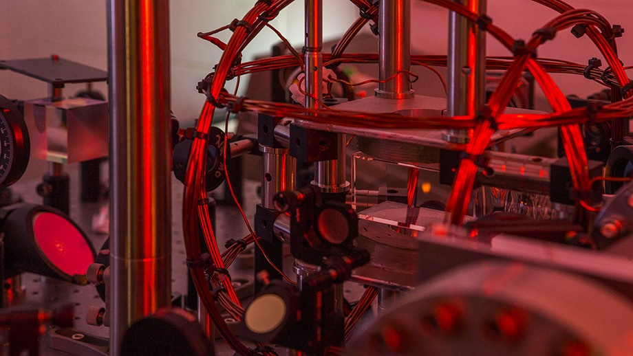
The experiment, featuring the small red glow of a BEC trapped in infrared laser beams (credit: Stuart Hay, ANU)
Australian physicists have used an online optimization process based on machine learning to produce effective Bose-Einstein condensates (BECs) in a fraction of the time it would normally take the researchers.
A BEC is a state of matter of a dilute gas of atoms trapped in a laser beam and cooled to temperatures just above absolute zero. BECs are extremely sensitive to external disturbances, which makes them ideal for research into quantum phenomena or for making very precise measurements such as tiny changes in the Earth’s magnetic field or gravity.
The experiment, developed by physicists from ANU, University of Adelaide and UNSW ADFA, demonstrated that “machine-learning online optimization” can discover optimized condensation methods “with less experiments than a competing optimization method and provide insight into which parameters are important in achieving condensation,” the physicists explain in an open-access paper in the Nature group journal Scientific Reports.
Faster, cheaper than a physicist
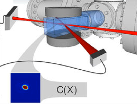
Optical dipole trap used in the experiment, showing the three laser beams and the condensate (red-yellow oval in blue square) (credit: P. B. Wigley et al./Scientific Reports)
The team cooled the gas to around 5 microkelvin. To further cool down the trapped gas (containing about 40 million rubidium atoms) to on the order of nanokelvin*, they then handed control of the three laser beams** over to the machine-learning program.
The physicists were surprised by the clever methods the system came up with to create a BEC, like changing one laser’s power up and down, and compensating with another laser.
“I didn’t expect the machine could learn to do the experiment itself, from scratch, in under an hour,” said co-lead researcher Paul Wigley from ANU Research School of Physics and Engineering. “A simple computer program would have taken longer than the age of the universe to run through all the combinations and work this out.”
Wigley suggested that one could make a working device to measure gravity that you could take in the back of a car, and the AI would automatically recalibrate and fix itself.
“It’s cheaper than taking a physicist everywhere with you,” he said.
* Billionth of a degree above absolute zero — where a phase transition occurs, and a macroscopic number of atoms start to occupy the same quantum state, called Bose-Einstein condensation.
** The 1064 nm beam is controlled by varying the current to the laser, while the 1090 nm beam is controlled using the current and a waveplate rotation stage combined with a polarizing beamsplitter to provide additional power attenuation while maintaining mode stability.
Abstract of Fast machine-learning online optimization of ultra-cold-atom experiments
We apply an online optimization process based on machine learning to the production of Bose-Einstein condensates (BEC). BEC is typically created with an exponential evaporation ramp that is optimal for ergodic dynamics with two-body s-wave interactions and no other loss rates, but likely sub-optimal for real experiments. Through repeated machine-controlled scientific experimentation and observations our ‘learner’ discovers an optimal evaporation ramp for BEC production. In contrast to previous work, our learner uses a Gaussian process to develop a statistical model of the relationship between the parameters it controls and the quality of the BEC produced. We demonstrate that the Gaussian process machine learner is able to discover a ramp that produces high quality BECs in 10 times fewer iterations than a previously used online optimization technique. Furthermore, we show the internal model developed can be used to determine which parameters are essential in BEC creation and which are unimportant, providing insight into the optimization process of the system.
The White House Office of Science and Technology Policy has announced plans to co-host four public workshops to spur public dialogue on artificial intelligence and machine learning, and to learn more about the benefits and risks of artificial intelligence, according to Ed Felten, a Deputy U.S. Chief Technology Officer.
These four workshops will be co-hosted by academic and non-profit organizations; two will also be co-hosted by the National Economic Council, with a public report later this year. They will be livestreamed:
The Federal Government also is “working to leverage AI for public good and toward a more effective government.” A new National Science and Technology Council (NSTC) Subcommittee on Machine Learning and Artificial Intelligence will monitor state-of-the-art advances and technology milestones in artificial intelligence and machine learning within the Federal Government, in the private sector, and internationally; and help coordinate Federal activity in this space.
The NSTC group also hopes to increase the use of AI and machine learning to improve the delivery of government services, especially in areas related to urban systems and smart cities, mental and physical health, social welfare, criminal justice, and the environment.
A simulation of Brownian motion (random walk) of a dust particle (yellow) that collides with a large set of smaller particles (molecules of a gas) moving with different velocities in different random directions (credit: Lookang et al./CC)
Researchers at the Universities of Bristol and Western Australia have demonstrated a practical use of a “primitive” quantum computer, using an algorithm known as “quantum walk.” They showed that a two-qubit photonics quantum processor can outperform classical computers for this type of algorithm, without requiring more sophisticated quantum computers, such as IBM’s five-qubits cloud-based quantum processor (see IBM makes quantum computing available free on IBM Cloud).
Quantum walk is the quantum-mechanical analog of “random-walk” models such as Brownian motion (for example, the random motion of a dust particle in air). The researchers implemented “continuous-time quantum walk” computations on circulant graphs* in a proof-of-principle experiment.
The probability distribution of quantum walk on an example circulant graph. Sampling this probability distribution is generally hard for a classical computer, but simple on a primitive quantum computer. (credit: University of Bristol)
Jonathan Matthews, PhD., EPSRC Early Career Fellow and Lecturer in the School of Physics and the Centre for Quantum Photonics, explained in an open-access paper in Nature Communications: “An exciting outcome of our work is that we may have found a new example of quantum walk physics that we can observe with a primitive quantum computer, that otherwise a classical computer could not see. These otherwise hidden properties have practical use, perhaps in helping to design more sophisticated quantum computers.”
Microsoft | Quantum Computing 101
* A circulant graph is a graph where every vertex is connected to the same set of relative vertices, as explained in an open-access paper by Salisbury University student Shealyn Tucker, including a practical example of the use of a circulant graph:
Example of a circulent graph depicting how products should be optimally collocated based on which products customers buy at a grocery store (credit: Shealyn Tucker/Salisbury University)
Abstract of Efficient quantum walk on a quantum processor
The random walk formalism is used across a wide range of applications, from modelling share prices to predicting population genetics. Likewise, quantum walks have shown much potential as a framework for developing new quantum algorithms. Here we present explicit efficient quantum circuits for implementing continuous-time quantum walks on the circulant class of graphs. These circuits allow us to sample from the output probability distributions of quantum walks on circulant graphs efficiently. We also show that solving the same sampling problem for arbitrary circulant quantum circuits is intractable for a classical computer, assuming conjectures from computational complexity theory. This is a new link between continuous-time quantum walks and computational complexity theory and it indicates a family of tasks that could ultimately demonstrate quantum supremacy over classical computers. As a proof of principle, we experimentally implement the proposed quantum circuit on an example circulant graph using a two-qubit photonics quantum processor.




 The White House Office of Science and Technology Policy has


